Sell Points
High beam uniformity
Low temperature etching
Introduction
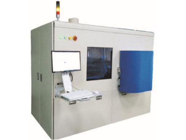
Ion beam etching is based on the sputtering principle, using the ion beam from the ion source to directly bombard the workpiece, sputtering out some materials on the workpiece that are not covered by the mask, so as to achieve the purpose of material removal.Ion beam etching is a pure physical etching process, which has the characteristics of the highest resolution and the best steepness in various conventional etching methods.
Feature
Workpiece table: circular rotation or scanning movement, adjustable etching angle, high etching uniformity, compatible with etching and polishing functions
The worktable is water-cooled to ensure low-temperature wafer etching
Plasma neutralizing gun can be configured to ensure no charge accumulation on the wafer surface
The Faraday beam measuring device can be configured to ensure the repeatability of process parameters
Vacuum system molecular pump / cryopump optional
Parameters
1. Worktable
Applicable chip size: 4 "~ 8", compatible with irregular square chip
Circular rotation / reciprocating scanning motion
2. Ion source: Kaufman ion source
Shape: round / bar
Ion beam energy: 0ev ~ 1000ev continuously adjustable
Beam current: 200mA (circular) or 300mA (bar) maximum
3. Etching uniformity: within ± 5% and between ± 3%
Application scope
It is used for polishing the substrate surface or material removal, especially for etching of metal material film, such as Cu, Au, Pt, Ti, Ni, NiCr, etc

